
 SPM Products > SPM Sample Images
SPM Sample Images
LT UHV SPM USM1200
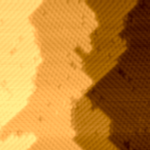
STM Topographic Image of Si (100)

Temperature: 63 K
Field of View: 3 nm × 3 nm
Dr. YOKOYAMA in Yokohama City Univ.
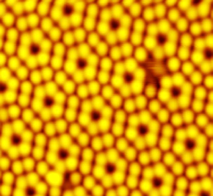
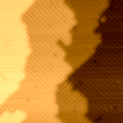
STM Molecular Structure and Topographic Image of COOH-Porphyrin-Tetramer
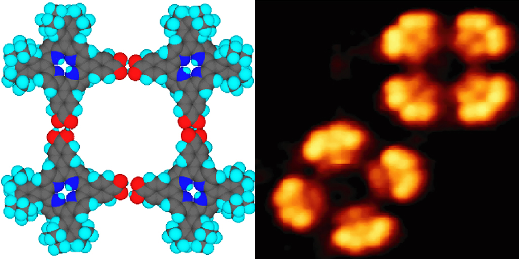
Temperature: 63 K
Field of View: 11 nm × 11 nm
Dr. YOKOYAMA in Yokohama City Univ.
3He LT UHV SPM with SC Magnet USM1300
STM Topographic Image of Si (111)
Tempetature: 4.2 K
Bias Voltage: 0.84 V
Tunnel Current: 1.04 nA
Field of View: 10 nm × 10 nm
Yutaka Miyatake, Unisoku Co., Ltd.
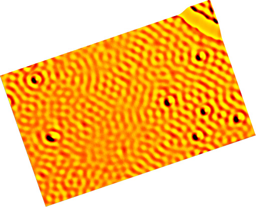
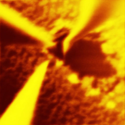
STM Topographic Image of Vortex Lattice of a Superconductor NbSe2
Temperature: 400 mK
Field: 0.5 T
Environment: UHV
Field of View: 250 nm × 250 nm
Dr. HANAGURI in Magnetic Materials Laboratory, RIKEN
STM Topographic Image and STS Data of Cleaved NbSe2

Temperature: 440 mK
Field of View: 7.3 nm × 7.3 nm
Dr. HANAGURI in Magnetic Materials Laboratory, RIKEN
Si (111) dI/dV Topographic Image in Magnetic Field (4.2 K, 7 T) USM1300 4He

Topo Image - Sample Bias 2.1 V Tunnel Current 1.24 nA

dI/dV Image - Sample Bias 1.2 V Tunnel Current 1.24 nA
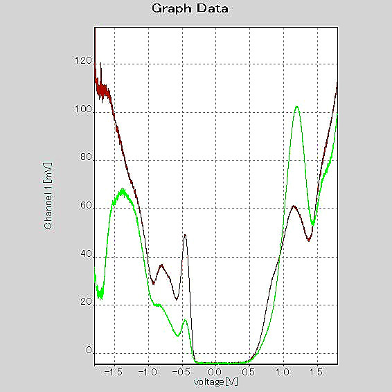
dI/dV-V curve on Si atoms
STM Topographic Image in 11 Tesla at 400 mK by USM1300 3He
Scan Size: 11.7
Sample bias: 2.07 V
Tunnel Current: 740 pA
Si (001) STM Topographic Image by USM1300 3He
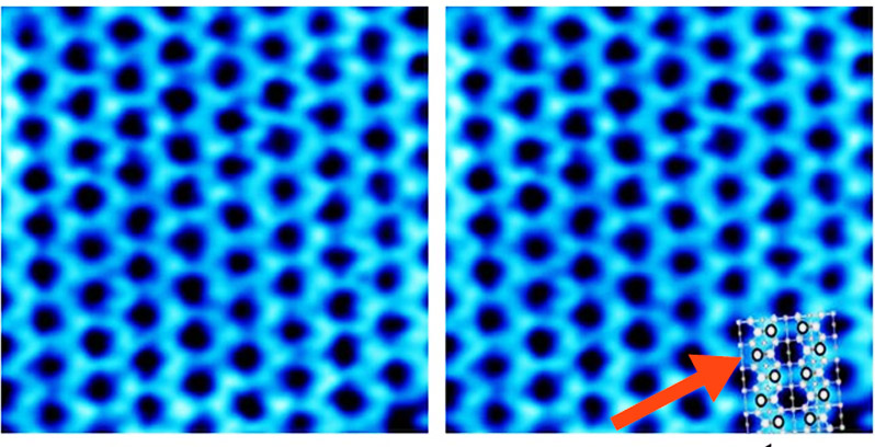
Add the atomic structure model
N type Si (100), 0.008–0.015 Ω cm
V = +1.7 V, I = 70 pA, 668.7 mK
Keisuke Sagisaka, NIMS, Fujita Group
published in VOLUME 91, NUMBER 14, 146103
PHYSICAL REVIEW LETTERS
Standing Wave on Cu (111) Surface by USM1300S VTI
Yukio Hasegawa Group, Univ. of Tokyo, Solid State Physics
VT UHV SPM USM1400
STM Topographic Image of Si (111) Surface
Temperature: 83 K
Scan Area: 22 nm × 22 nm
Sample Bias: 1.8 V
Tunnel Current: 0.54 nA
UNISOKU Co., Ltd.
STM Topographic Image of Si (100) Surface

Temperature: 83 K
Scan Area: 12 nm × 5 nm
Sample Bias: 1.2 V
Tunnel Current: 1.0 nA
UNISOKU Co., Ltd.
Temperature: 83 K
Scan Area: 20 nm × 20 nm
Sample Bias: -2 V
Tunnel Current: 0.2 nA
UNISOKU Co., Ltd.
Temperature: 83 K
Scan Area: 20 nm × 20 nm
Sample Bias: 2 V
Tunnel Current: 0.2 nA
UNISOKU Co., Ltd.
VT UHV 4-Probe SPM USM1400-4P
4 Point Measurement
UNISOKU Co., Ltd.
STM Image on HOPG at 6.5 K

UNISOKU Co., Ltd.
Resistance of Micro Structure

UNISOKU Co., Ltd.
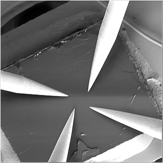
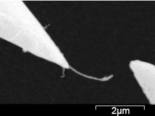
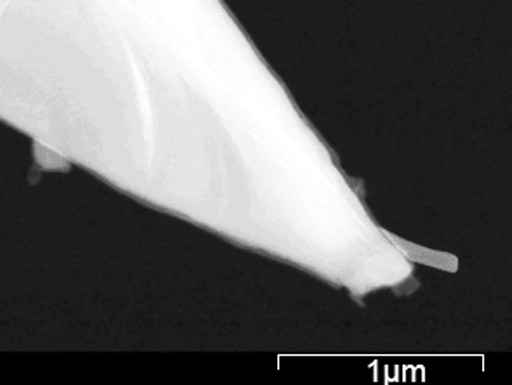
4-Nano-Probe System for SEM UMP-1000
Four Probes Over Carbon Nanotube

Four-terminal Resistance measuremaent on Carbon Nanotube
Probe distance: < 10 µm
Prof. Sumiyama, Nagoya Institure of Technology
SEM Image of 4 Probes below 10 K
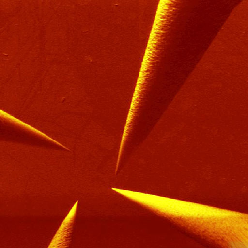
Scan Area: 1 mm × 1 mm
Temperature: 6.5 K
UNISOKU Co., Ltd.
Scan Area: 15 µm
Temperature: 6.5 K
UNISOKU Co., Ltd.
Cutting CNT by 2 Probes
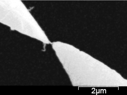
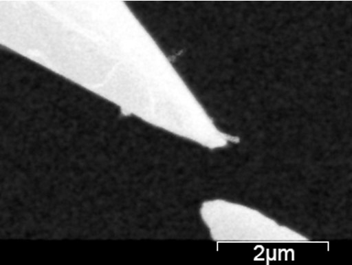
Applying a voltage across the probes
M. Yoshimura, Ueda Lab., Toyota Technological Institute
Advanced HV-STM System HS-1000
STM Image of Mn Porpyrin Molecules on Au (111)

Scan Size: 10 nm × 10 nm
Sample Bias: 1.2 V
Tunnel Current: 10 pA
UNISOKU Co., Ltd.
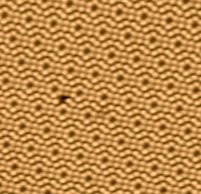
STM Image of Au (111) Herringbone Structure
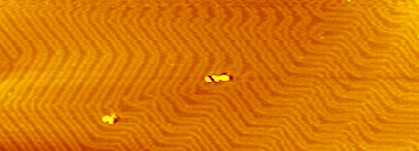
Scan Size: 180 nm × 90 nm
UNISOKU Co., Ltd.
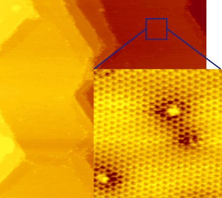
STM Atomic Image of Si (111) 7 × 7 Structure
Scan Size: 12.8 nm × 5.1 nm
UNISOKU Co., Ltd.
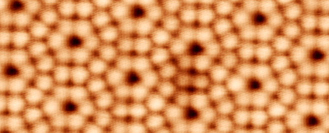
STM Atomic Image of √3 × √3 - Ag Structure on Si (111)
Scan Size: 12 nm × 12 nm
Sample Bias: -0.4 V
Tunnel Current: 0.7 nA
UNISOKU Co., Ltd.
Extreme Physical Fields Scanning Probe Microscope
AFM Topographic Image of Si (111) Surface
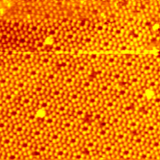
Figure: Si (111) 7 × 7 by NC-AFM
Scan Size: 13 nm × 13 nm
Cantilever: Piezo Resistive type (made by SII)
Frequency shift: -33 Hz
Ichiro Shiraki, NIMS, Miki group