

USM1400-4P
PDF
SPM System Specs.
Published Papers
PDF SPM System Specs. Sample Data
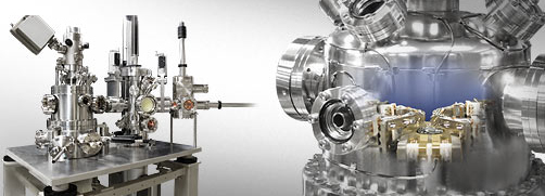
The most multifunctional commercial system.
Deriving benefit of high performance multi probe SPM system, this new tool is actively used in nanotechnology research.
Undertook the project from JST development of advanced measurement and analysis systems, UNISOKU developed the latest multi probe microscope system with all its might for the first time in the world. This system is used for devices evaluation and micro/ nanoscale surface electrical conductivity measurement in wide temperature range including ultra low temperature using probe scanning microscope with four independently controlled probe.
Realizing high resolutions using multi probes developed in house, enabling wide range application measurement.
Features
- Nanoscale positioning possible using SEM
- Each four probe has STM/AFM functions
- Four-terminal conductivity measurement by nanoscale
- Ultra high vacuum chamber for MBE
- Ready for photo irradiation, emission measurement, high frequency measurement
- Hole effect, spin measurement applicable using super conducting coil (optional)
Applications
- Four terminal resistivity measurement of conductive thin film by micro or nanoscale
- Conductivity measurement of nanostructure and nanodot
- Temperature dependence measurement of conductivity for organic conducting layers and semiconductors
- Local electrical characteristic analysis of nanodevice
- STM imaging at various temperature
- Wide application for surface analysis
Specifications
| Four probe STM Head | |
|---|---|
| MAX scan range (X × Y × Z) | 0.38 × 0.38 × 0.38 µm3 @ 5 K |
| Minimum resolution (STM) | X, Y: 0.1 nm (Atomic resolution) Z: Under 0.02 nm |
| Sample and probe stage | MAX range X, Y: 5 mm; Z: 3 mm |
| FE-SEM | |
| Minimum resolution | 20 nm (acceleration voltage 25 kV, WD 15 mm, probe current 1 nA) MAX field of view 3 mm × 3 mm (acceleration voltage 5 kV) |
PDF SPM System Specs. Sample Data