
 SPM Products > Time-resolved scanning tunneling microscopy system
Time-resolved scanning tunneling microscopy system
PDF (Brochure)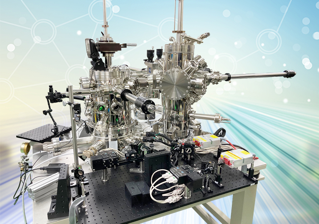
✔Collaboration with Prof. Shigekawa group (University of Tsukuba)
✔This project was supported by A-STEP, JST.
Features
Compact optical pump-probe system
●Temporal resolution ~ 80 ps
●Easy operation & maintenance
●Stable laser illumination on sample surface
●Integration into an existing STM system possible
※The optical system alone can be purchased.
Nanoscale carrier dynamics measurement
●Spatial resolution ~ 1 nm
●Long-term time-resolved measurements (~ 1 day)
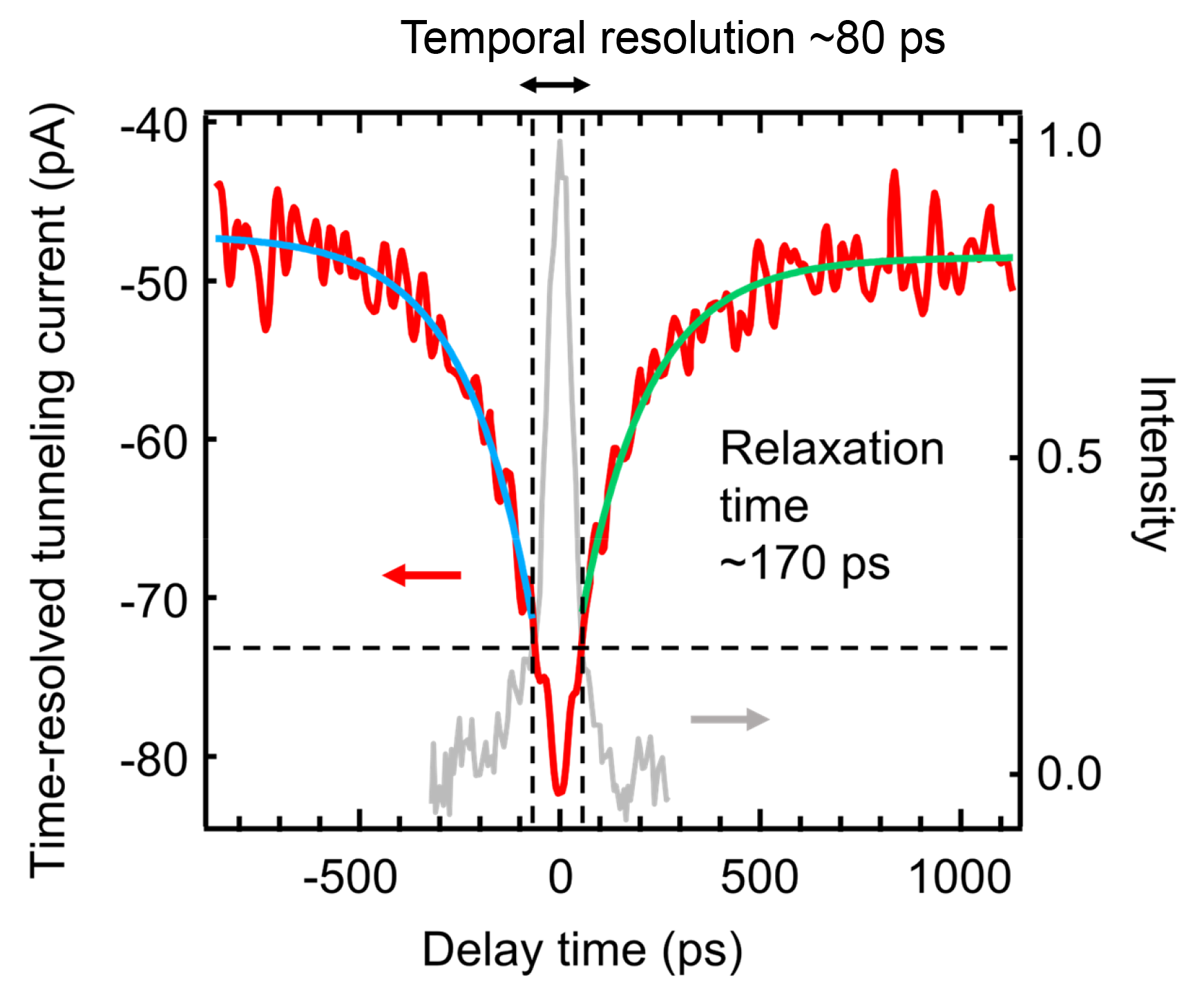
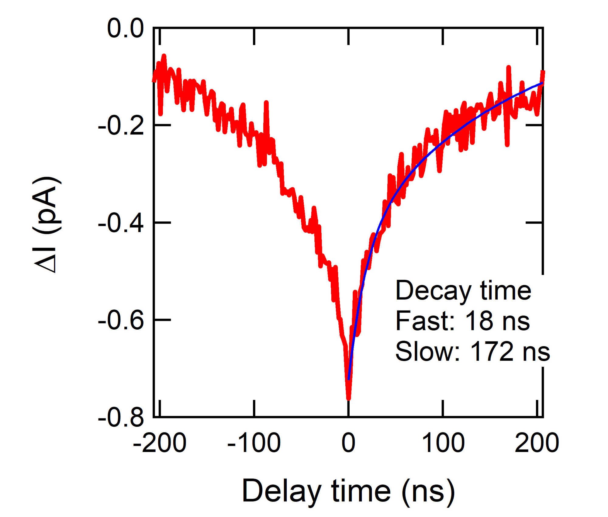
Performance test1:Time-resolved tunneling current of low temperature grown GaAs (T = 300 K)
|
Performance test2:Relaxation time mapping of GaAs(110) surface (T = 6 K)
surface_EN.png)
|
Applications
●Semiconductor surfaces, heterostructures
●Transition metal dichalcogenides
●Photocatalytic materials
●Solar cell materials, etc.
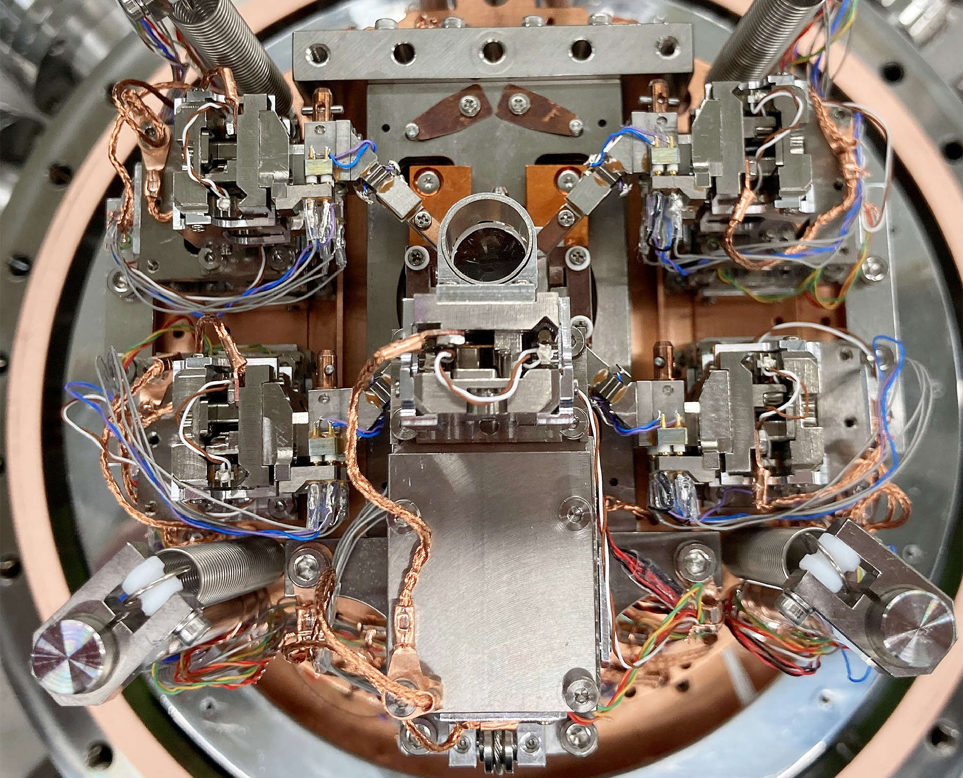
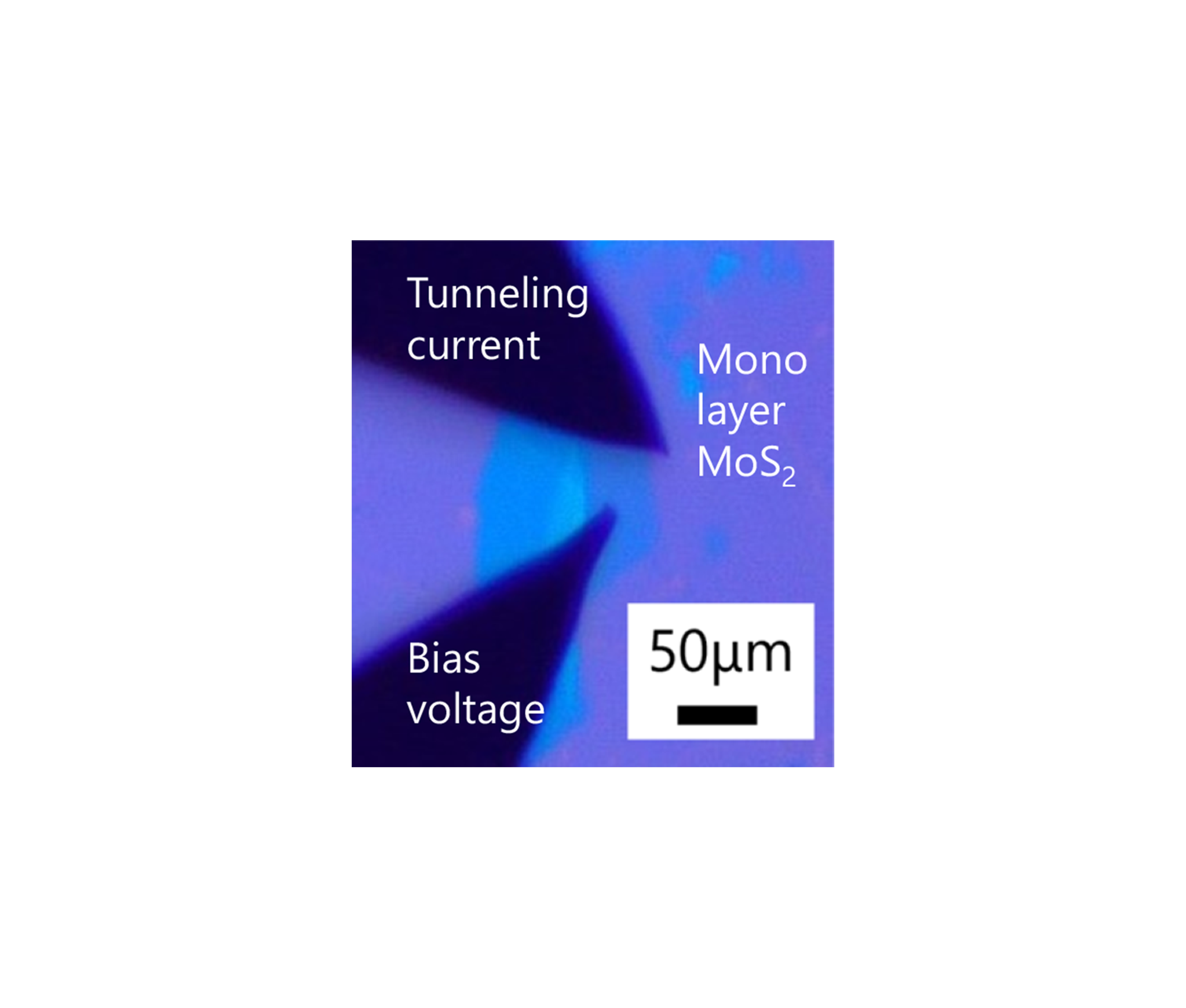
Time-resolved multiprobe microscopy system
|
Carrier dynamics measurement of micro samples on insulating substrate
●Sample and probe observation using a long-focus microscope Demo measurement conditions
●Temperature: 77 K or 300 K |
|
|