

Conductive Nanoprobe for Probers
Nickel, Platiniridium Probes
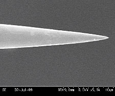
SEM Image of Tungsten Probe Tip
Micro and nano scale multi-probing techniques are used in semiconductor device R & D and production of probe sample surfaces, as when measuring the surface electrical characteristics for failure analysis. With the increasing intricacy of device structures in recent years, higher demands on probe specifications has arisen. That is, to increase sharpness and controllability of surface oxide films. Demand for such probes is also getting larger in various other fields, including nanobiology. To meet these needs, UNISOKU has developed contact inspection nanoprobes for a variety of applications.
Line-up of Conductive Nanoprobe for Probers
Small Tip Angles Produce Better Tip Shapes for Multi-Probe Applications
Probe tips are shaped with a small tip angle so that probes can be placed close together at acute angles without interrupting one another.
Capable of Soft Contact with Samples*1
Without an intervening surface oxide film, Nickel probes and Platiniridium probes can quickly achieve conductivity on contact, minimizing damage to samples and probes.
*1: Applies to Nickel probes and Platiniridium probes and NOT to Tungsten probes.