

UMP1000-4P NanoProber (UHV)
PDF
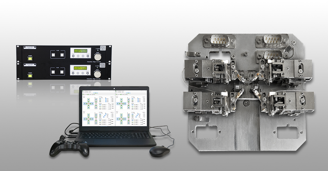 Controller Electronics
Notebook PC
Nano Probe Unit
Controller Electronics
Notebook PC
Nano Probe Unit
* 0.1 nm resolution is possible with optional software.
PDF
Controller Electronics
Notebook PC
Nano Probe Unit
Features
- This system is installed in SEM stage and measures 4 point local electric conduction in submicron area.
- Each probe position can be controlled in 3 dimensional directions in nanometer resolution by control circuits with notebook PC.
Specifications
| XY Range | |
|---|---|
| Coarse | ±3 mm in ±150 nm steps |
| Fine | ≤1 μm in 10 nm* steps |
| Z Range | |
| Coarse | ±1.5 mm in 150 nm steps |
| Fine | ≤1 μm in 10 nm* steps |
| Sample Size | 10 mm × 10 mm × 1 mm |
| Weight | ≤1000 g |
Basic Components
| Components | H/W/D (cm) Approx. |
|---|---|
| Nano Probe Unit | 36 / 116 / 116 |
| Controller Electronics | 88 / 430 / 350 × 2pcs |
| Notebook PC | A4 size or B5 size |
| Pt:Ir Probe | - |
| Accessories | - |